1. Integrated Circuits: A Brief History
The semiconductor industry can trace its roots back to the invention of the first semiconductor transistor by William Shockley, John Bardeen, and Walter Brattain at Bell Labs in 1947.1 Their crude device was assembled from a small piece of germanium, some gold foil, a paper clip, and several pieces of plastic. Though crudely constructed, it performed its function of using a voltage to switch an electrical current on or off quite well. This simple device is the parent of all of the various semiconductor transistor devices produced over the years, including computer microprocessors, memory chips, and solid state power amplification circuits.
The new transistor found a home in a number of markets where it could replace bulky and troublesome vacuum tubes (radios and televisions), and it created new markets that were invented specifically to exploit its use. The discrete transistor was quickly incorporated in everything from telephone equipment to pocket-sized transistor radios. It is interesting to note that the size of the parts in these early discrete devices were on the order of tenths of an inch. By the late 1950s, the discrete transistor market was worth an estimated $1 billion annually.1
The next major step in semiconductors was the invention of the first monolithic integrated circuit by Jack Kilby and Robert Noyce in 1960.2 Their integrated devices consisted of many solid-state transistors that were manufactured and interconnected internally on a single semiconductor substrate. The typical minimum feature size in these early products was greater than 20 mm, significantly smaller than some of their discrete transistor counterparts. The ability to interconnect the devices internally allowed more complex functions to be performed by a single device. Interconnection also made it possible to pack a larger amount of function into areas far smaller than was possible with discrete transistors. It was the invention of the "integrated circuit" that ushered in the modern microelectronics era, and it is still adaptations of that basic product that fuel the semiconductor industry.1-3
Significant progress has been made since 1960, when device features were approximately 20 mm wide. Todays leading edge semiconductor devices have critical dimensions as small as 0.18m m. The term critical dimension, as used in semiconductor parlance, commonly refers to the smallest circuit element in the device or on a particular level of the device. In comparison, the diameter of a human hair is approximately 50 mm and typical bacteria are on the order of 5 mm in size (see Figure 1.1). It has been this ability to continue to shrink the dimensions of the patterns in semiconductor devices that has driven the dramatic progress in the industry. Reductions in feature sizes allow more devices to be integrated onto a single chip, which in turn results in more functionally powerful products. One interesting fact is that while the feature sizes have decreased and the number of structures in integrated devices have increased, the overall cost of making a semiconductor device have remained reasonably constant.2 This has led to a dramatic increase in the function per cost for semiconductor devices. Reductions in the feature sizes, especially in the size of transistor gate structures (see Figure 1.2), have also led to dramatic increases in the speed of logic devices such as microprocessors.2
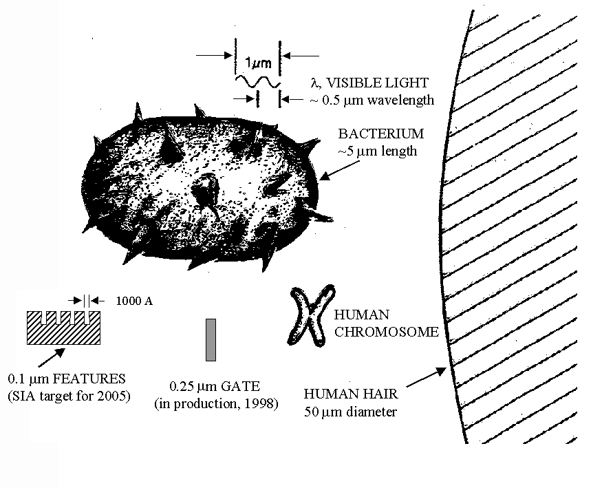
Figure 1.1: (Above) Relative size of various objects in relation to modern semiconductor
device features.4
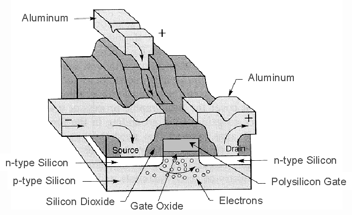
Figure 1.2: (Below) Schematic representation of a single semiconductor transistor device.
Application of a voltage to the gate allows current flow between the source
and drain of the transistor.2
This ability to manufacture smaller features has been enabled
mainly by advancements in lithographic technologies.2,4-6 Photolithography,
lithography, or microlithography is the art and science of printing the
circuit element patterns used for the construction of semiconductor devices.
Figure 1.3 shows a schematic representation of the overall process flow
in the manufacture of integrated circuit devices.3,6 Single
crystalline silicon wafers are manufactured from raw polysilicon
for use as substrates for the various semiconductor devices. The integrated
circuits are then manufactured by repeatedly processing the substrates
through a cycle of three basic unit operations: film deposition, lithography,
and etch. This cycle builds up the patterned layers (semiconductors, conductors,
and insulators) required to make a final device. The overall cycle may
be repeated as many as 20 to 30 times for modern logic devices. In general,
each material, such as metallic conductors or insulators, is deposited
as a blanket film over the entire substrate. The substrate is then covered
with a protective polymeric material, the photoresist,
that can be patterned in the lithographic step to provide patterned access
to the underlying film. The patterned photoresist
layer is used as a protective mask for an etch process that selectivity
removes undesired areas of the underlying film. After the etch process
is complete, the photoresist layer is stripped
away and the process is repeated to build up the various layers. In this
way, it is the resolution of the lithographic and etching processes that
controls the minimum feature size of the patterns in finished semiconductor
devices. Consequently, there is an ever increasing desire to make advancements
in the lithographic technologies used in semiconductor manufacturing,
since these advancements are required to allow the industry to continue
to move forward.3

Figure 1.3:
Simplified overall process
flow for the manufacture of semiconductor integrated devices.
2. The Lithographic Process
The manufacture of semiconductor products requires the ability
to work selectively on small, well-defined areas of the semiconductor
substrate. The process by which these well-defined areas are patterned
is again known as the microlithographic process.2-5
The basic steps in the lithographic process are shown in Figure 1.4. The
first step in the process is the preparation of the substrate. This step
usually involves cleaning the surface through various solvent and plasma
cleaning procedures. The surface may also be treated using a prime step,
in which it is exposed to a reagent, such as hexamethyldisilizane
(HMDS), that modifies the surface chemistry of the substrate to improve
the adhesion of the photoresist to the surface.
In the next step, a material known as a photoresist
is applied. The photoresist is a material that
undergoes a change in its physical and/or chemical properties upon exposure
to radiation that allows for the formation of a relief pattern in the
material. The resist, in the form of a solution in an organic solvent,
is spin coated onto the substrate and then soft baked (SB) on a hot plate
or in an oven to remove residual casting solvent. The desired product
from this step is a uniform, glassy, polymeric thin film that is generally
on the order of 1 mm thick. The resist coated substrate is then exposed
patternwise to radiation, typically ultraviolet
light. The exposure tool uses a mask to selectively expose the desired
pattern into photoresist. Following exposure,
the resist is typically post-exposure baked (PEB) on a hot plate or in
an oven. This bake step serves a number of different purposes that will
be described later. The resist is then treated with a developing solvent,
by immersion or some other technique, that selectively dissolves either
the exposed or unexposed areas depending on the nature of the resist.
The areas of the substrate that are no longer covered by photoresist
can then subjected to further processing such as plasma etching or ion
implantaion. The remaining resist patterns serve as a barrier
that protects the underlying substrate from these processes. Once the
substrate is processed, the photoresist layer
is stripped and the entire process is repeated for each layer of the device.
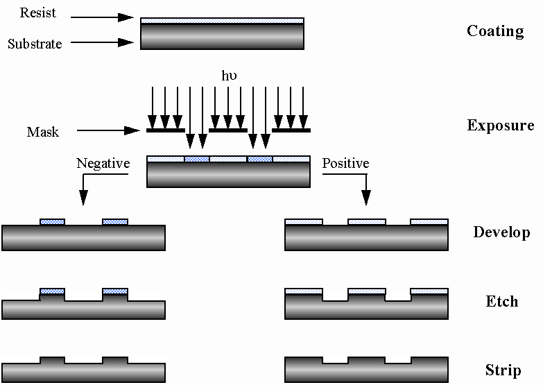
Figure 1.4: General schematic of the steps in the
lithographic process.
The reduction in the minimum feature sizes in semiconductor
devices has been made possible over the years by a continuous progression
of advancements in the lithographic technologies used to pattern the devices.2,5,7
Figure 1.5 shows the progression of memory technologies over the past
25 years, along with projections of future technologies. The plot also
shows the lithographic technologies used to manufacture each device generation.
One of the main ways to reduce the device critical dimensions has been
to continually reduce the wavelength of the radiation used to expose the
photoresist.
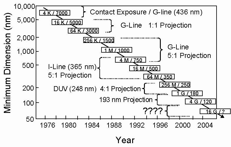
Figure 1.5: Semiconductor industry roadmap of memory
technologies and the associated lithographic technologies used to the
manufacture of each device generation. Each box shows each device generations
memory size and critical feature size (nm).
The resolution of a diffraction limited lithographic process is given by the Raleigh criterion as shown in equation (1.1), where l is the wavelength of radiation used, NA is the numerical aperture of the lens in the projection tool exposure system, and k1 is a process dependent adjustment factor. The k1 factor is controlled by a variety of things including the photoresist performance and tool issues such as lens aberrations.5,8
Resolution ![]() (1.1)
(1.1)
The numerical aperture is defined as the sine of the capture angle of the lens, and is a measure of the size of the lens system. All of these factors are under attack in the race to print smaller features. Exposure tool manufacturers are developing lens systems with higher numerical apertures. Semiconductor manufacturers, aided by resist makers and other tool suppliers, are learning to manufacture with lower k1 factors. Reducing the exposure wavelength has demanded a series of advancements in the corresponding photoresist technologies used for each process. As the exposure wavelength is decreased, new resist materials that are sensitive to these lower wavelengths must be developed. In any given wavelength generation, improvements made in the exposure tool technologies and resist performance can allow for reductions in the minimum printable critical dimensions. A more detailed description of photoresists is required to further understand this point.
Photoresists are traditionally polymeric materials which can be either
single or multiple component formulations. The simplest resists are single
component materials such as poly(methyl methacrylate),
or PMMA, which is used as a resist in electron beam lithography. Under
exposure to electron beam radiation, the PMMA polymer undergoes chain
scission that reduces the molecular weight of the material. This reduction
in molecular weight causes the PMMA to dissolve orders of magnitude faster
in the appropriate developing solvent, resulting in the ability to pattern
the resist.4,5
The majority of resists used in semiconductor production
today are multi-component formulations. In general, these multi-component
resists can be classified as either non-chemically amplified (diazonaphthoquinone-novolac type resists) or chemically-amplified
(CA).4,5 The basic operation of these two types of resists
is shown in Figure 1.6. The diazonaphthoquinone-novolac,
or DNQ-novolac, resists have been the workhorse
for the semiconductor industry for over 20 years and continue to be the
most widely used resist technology in high volume semiconductor production
today.5 DNQ-novolac resists are used
with several different exposure wavelength technologies: I-line (365 nm),
G-line (436 nm), and broadband (380-450 nm). The choice of these exposure
wavelengths arises from the fact that mercury arc lamps are used as the
light sources in the exposure tools for these resists. During the early
development of Deep-Ultraviolet (DUV) lithography at 248 nm, the only
available and practical light source was still a mercury arc lamp. However,
the output of the mercury arc lamp light sources is very low at this wavelength.
Therefore, productivity requirements demanded the development of more
sensitive resists, resulting in the invention of chemically-amplified
resists.4 Chemically amplified resists will be the resist technology
of choice for the next several generations of lower wavelength lithographic
technologies. However, DNQ-novolac resists are
still by far the most widely used photoresists.
Advancements in these materials and the processes used to image them have
extended their use to printing features as small as 0.25 mm. There are
also large and growing markets for these resists in the form of thick
film materials for use in the manufacture of thin film magnetic heads
and other microstructures, including micromachines.
The focus of this research has been on the modeling and characterization
of DNQ-novolac photoresists.
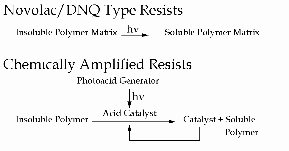
Figure 1.6: Comparison of chemically amplified and
non-chemically amplified resist function.
Photoresists are also classified as positive or negative tone materials (see Figure 1.4). In a positive tone resist, the areas that are exposed to the radiation develop away into solvent faster than unexposed areas, resulting in a positive tone image of the mask. The majority of commercial, positive tone, non-chemically amplified resists used today are variations on the well-known, two component, diazonaphthoquinone-novolac resists. Novolac is a name generally given to acid catalyzed phenol-formaldehyde condensation polymers of the type shown in Figure 1.7. Commercial resists often contain novolac made from a feed that is a complex mixture of meta-cresol, para-cresol, and other additives.5
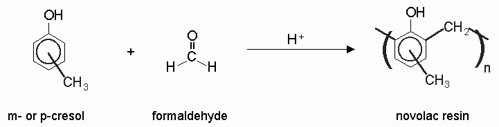
Figure 1.7: Commercial production of novolac resins is typically accomplished via the acid catalyzed
polymerization of cresols with formaldehyde.
Novolac polymers are soluble in a variety of common organic solvents.
Resist films are typically cast from organic solutions (propylene glycol
monomethyl ether acetate, or PGMEA, is a common
solvent) to form isotropic, glassy, thin films. These polymers are also
soluble in aqueous base due to the presence of the acidic phenolic
functionalities on the polymer backbone. It is this base solubility that
is exploited in the development process. In order to print a relief image
in a photoresist it must be possible to modify the dissolution
rate of the resist upon exposure to radiation. It is not the novolac polymer in DNQ-novolac resists
that is sensitive to radiation. Instead, it is the second component of
the resist, the diazonaphthoquinone (DNQ), that
is responsible for the ability of the resist to change its dissolution
behavior upon exposure to radiation. DNQ is often referred to as the photoactive
compound (PAC) or sensitizer in the resist, since it is the component
which responds to radiation exposure. Thus, the role of the novolac
polymer in these resists is to provide the desired physical characteristics
of the material, such as good film forming properties and etch resistance
to plasma processing, while the DNQ allows the resist to be imaged. Figure
1.8 shows a schematic view of the basic mechanism responsible for the
function of DNQ-novolac photoresists.5
Figure 1.8: Schematic picture of the mechanism by
which DNQ-novolac resists function.
The addition of diazonapthoquinones
to novolac films leads to a reduction in the
dissolution rate of the polymer film in aqueous base relative to the dissolution
rate of the pure polymer. This difference in rate can be as large as several
orders of magnitude. Diazonaphthoquinone is
therefore termed a dissolution inhibitor due to its ability to retard
the dissolution rate of the novolac film. As
shown above, DNQ undergoes a series of reactions upon exposure to radiation
to form a carboxylic acid product. This carboxylic acid, unlike the hydrophobic
DNQ, is soluble in aqueous base and its presence in the polymer film does
not retard the dissolution rate in aqueous base. In fact, the presence
of the carboxylic acid often serves to increase the dissolution rate of
the novolac several orders of magnitude relative
to the pure novolac polymer. It is this change
in the dissolution rate of the novolac film
due to the reaction of the diazonaphthoquinone
with light that allows for the formation of relief images in the resist
film.5
Despite their heavy use in industry, there is a general
lack of a fundamental understanding of the molecular level mechanisms
and interactions that underlie the function of DNQ-novolac
photoresists. This lack of fundamental knowledge
has made the rational formulation of new resists difficult. In general,
the design of new resists is more of an art than a science. This lack
of understanding has also made modeling and simulation of the function
of this type of photoresist difficult.
Lithography simulation, which will be discussed in more
detail in the next section, is becoming an increasingly important tool
for the semiconductor industry. It is used in a variety of tasks including
process optimization and device ground rule generation. Difficulty in
modeling the performance of DNQ-novolac photoresists
has somewhat limited the usefulness of these simulation techniques. The
goal of this research has been to contribute to the fundamental understanding
of the molecular level mechanisms by which DNQ-novolac
resists function and to contribute to the state of the art in modeling
and simulating their performance.
3. Lithography Simulation
Lithography simulation and modeling refers to the ability
to simulate the output of various stages of the lithography process using
a set of physical process parameters and a set of descriptive models.9-12
This simulation process will be discussed in greater detail in the following
sections. However, before considering the details of lithography simulation,
let us consider the advantages and uses of this technology.
Lithography simulation is growing in importance within the
semiconductor industry. There are several reasons for its value. One of
the dominant reasons relates to the cost and time required to perform
experiments in a semiconductor fabrication facility (fab).10
Product cycle times in the semiconductor industry are relatively short
(between 1 and 2 years). This pace puts severe limitations on the amount
of time that can be spent on research and development for each new product
line or manufacturing process. A simulation experiment for optimizing
the optical proximity correction features (see Figure 1.9) for a new mask
set may only take one day. A similar optimization using experiments on
wafers might take a month from the time the test mask designs are generated
until wafers are finished and metrology results are generated. Any savings
in time that can be realized through the use of simulation is very valuable.
The cost of experiments on wafers in a semiconductor fab
are staggering. A box, or lot, of 25 wafers containing microprocessors
such as the Intel PentiumÔ or Motorola PowerPCÔ is
worth approximately $2 million when finished. Therefore, research and
development activities in the fab use valuable
time and wafers that could be utilized to make products. Any increase
in the number of wafer starts that can be used for production rather than
research and development activities presents quite a large financial benefit.
Lithography simulation provides the opportunity to perform experiments
in a virtual environment that can be both much faster and cheaper than
full-scale wafer level experiments.
There are a number of areas in which lithography simulation
tools are valuable, including circuit design ground rule generation, optical
proximity correction (OPC), and exposure tool optimization.10,13-15
Each semiconductor device is designed using a set of ground rules that
state the guidelines and specifications which must be met in the design
in order for it to perform properly and to insure that the device is manufacturable.
An example of a common ground rule is the minimum feature size that can
be used on a design. Another interesting area in which lithography simulation
is finding widespread use is in the process known as optical proximity
correction (OPC). The basic idea in OPC is to correct for distortions
in the final printed image relative to the original mask design that are
introduced by optical distortions in the exposure tool and other various
processing effects (see Figure 1.9).
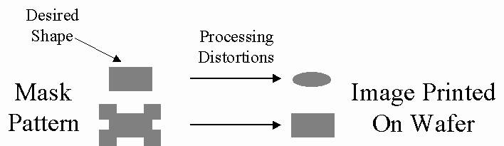
Figure 1.9: Schematic view of principle behind optical
proximity correction (OPC). The mask design is distorted in such a way
as to print the desired feature shape, negating the effect of processing
distortions.
These distortions can lead to a variety of problems including
poor device performance, failure, or reliability problems depending on
their nature. The mask pattern is altered during its design in such a
way as to allow for the final printed image to match the desired pattern
shape. Lithography simulation can be used to predict the distortions introduced
by the exposure tool optics and thereby allow the mask design to be altered
without ever printing a wafer. Until recently, it was not possible to
simulate final resist profiles with sufficient accuracy to make OPC corrections
due to the difficulties associated with resist performance modeling. Instead,
OPC corrections had to be performed using only aerial image simulations.
In other words, only the distortions due to the propagation of light through
the lens systems have been simulated, thus ignoring the effects of resist
chemistry and processing. This is one obvious area in which improving
resist modeling capability could have a large impact. Another area in
which lithography simulation is finding widespread use is in the optimization
of exposure tool settings. The lithography process engineer has a number
of parameters, such as the numerical aperture of the lens system and the
partial coherence of the light source, that can be adjusted on an exposure
tool to improve its imaging performance. Since the optics of the exposure
tool can be modeled rigorously, it is a simple matter to test the effect
of changing these parameters using simulation. Improvements in the area
of resist performance modeling would help the accuracy and utility of
such simulations.
For the purpose of modeling, the lithographic process can
be broken down into two distinct stages. The first step is the exposure
of the photoresist and the generation of the latent image.4,5,9,11
The latent image is the concentration, or reaction, profile set up in
the resist due to exposure to radiation. The second step is the development
process in which the latent image is developed to produce the desired
relief image. This is a somewhat simplified picture since the bake steps
in lithographic processing result in changes in the resist properties,
especially in chemically amplified resists.
One can further break the exposure process down into two
separate steps that can be modeled independently: aerial image formation
at the resist surface and exposure (propagation of radiation and reaction
within resist layer) of the resist.10 Thus, the lithographic
process can be broken down or subdivided into three general steps as shown
in Figure 1.10: formation of the aerial image, exposure of the resist,
and the development step. A more detailed breakdown of the lithography
process and the various steps in lithography simulation is shown in Figure
1.11.
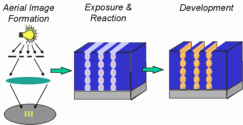
Figure 1.10: (Above) The three basic steps of the lithographic
process from a lithography modeling viewpoint.
Figure 1.11: (Below)
Detailed breakdown of the lithographic process from the viewpoint of simulation.
The left column entries show examples of the required physical parameters.
The illustrations at the right show a pictorial schematic of the result
of each step.
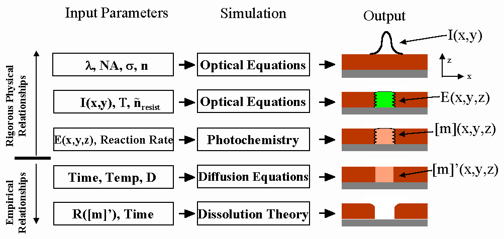
The aerial image is the intensity distribution that results
from projecting the image of the mask onto the wafers surface. The aerial
image can be described as the intensity of radiation as a function of
position at the surface of the wafer plane, I(x,y).
A number of different technologies can used to generate this aerial image
including contact, proximity, and projection printing. A description of
each of these technologies and their associated variations is beyond the
scope of this work but can be found in a number of reference materials.8,16
Today, projection printing is by far the most commonly used exposure method.
In projection printing, a complex lens system is used to focus an image
of a mask onto the surface of the substrate (see Figure 1.12). One of
the main advantages of these projection tools is the opportunity to use
reduction lens to produce images on the wafer that are smaller than the
actual dimensions of the images on the mask. This reduction capability
is very important, since it eases the specifications of the features sizes
on the mask, thus allowing masks to be made at lower costs.
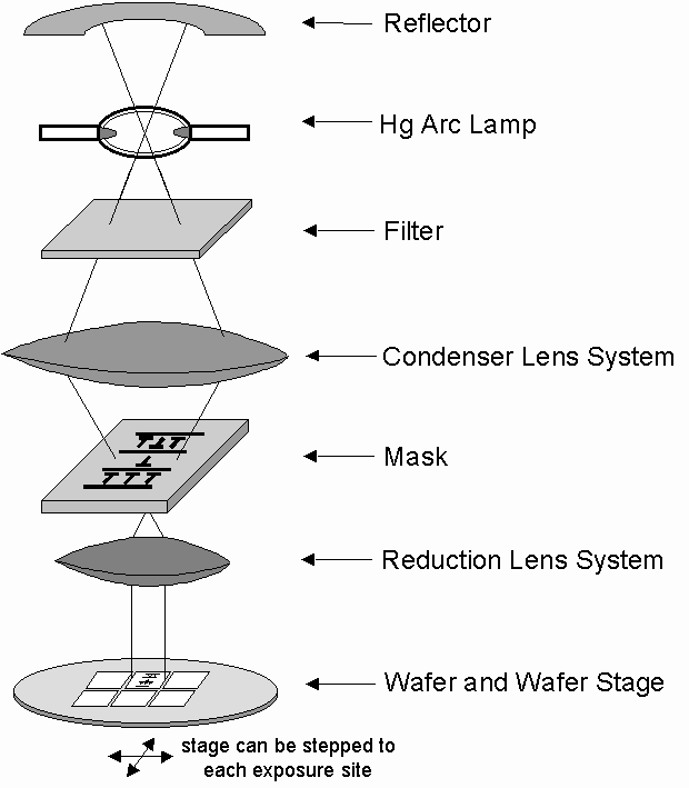
Figure 1.12: Schematic of simplified step-and- repeat
projection exposure tool system. This system shows the configuration
of a typical I-line tool that uses of a Hg arc lamp source. New DUV systems
generally use excimer laser sources.
Modeling the aerial image generated by an exposure system
is a rigorous and well understood procedure that requires a knowledge
of the optics of the complex lens systems in the exposure tool. This simulation
can be accomplished using standard Fourier optics descriptions of the
process. The end result of this simulation step is the intensity distribution
at the wafer plane, I(x,y).
The propagation of light in the resist, and the resulting reaction of the photoactive compound (PAC) is a somewhat more complex process. These two processes are coupled since the propagation of light causes the PAC reaction to proceed which results in a change in the composition of the resist material.11 This changing composition in turn affects the manner in which the light propagates in the resist. There are three sets of physical parameters that are required to model this process of light propagation and reaction within the resist: the refractive index as a function of wavelength, the resist absorption properties, and a rate constant for the PAC reaction with light. The refractive index is used in conjunction with the absorption properties of the resist to predict the intensity distribution within the resist due to the propagation of radiation within the resist film stack. The rate expression for the PAC reaction is used to model the changing composition of the resist during the exposure process. One of the major goals of this work has been to develop techniques that allow for the rigorous characterization of the refractive index behavior, absorption properties, and reaction rates of non-chemically amplified photoresist systems. The desired end result of the simulation of the exposure process is a knowledge of the concentration distribution of the PAC within the resist, [PAC](x,y,z) or m(x,y,z).
The last step in the lithographic process is the development
of the exposed resist layer to form the final relief image patterns. A
rigorous description of this process would require a fundamental knowledge
of the various mechanisms that control the dissolution rate of the photoresist in its developing solvent. This basic knowledge
is missing for both DNQ-novolac and chemically
amplified resists. There is still no comprehensive theory that captures
all aspects of the resist development process. One of the goals of this
work has been to contribute to developing a more comprehensive model for
the dissolution behavior of novolac polymers.
In the absence of such a fundamental understanding, empirical relationships
must be used to model the development of photoresists
in lithography simulation.10,11,17-19 The development rate
of the resist is simply described and modeled as a function of the remaining
PAC concentration after the exposure process. In this work, new techniques
for extracting these relationships between development rate and PAC concentration
for DNQ-novolac photoresists have been developed.
Click here for a Schematic of the Lithography process
4. References
- M. Riordan, L. Hoddeson, Scientific
American, Special Issue "The Solid-State Century," 10,
(1997).
- L.F. Thompson, "An Introduction to Lithography,"
Introduction to Microlithography, Second Edition, Ed. L.F. Thompson,
C.G. Willson, and M.J. Bowden, Washington,
DC: American Chemical Society, 1, (1994).
- C.R. Barrett, Scientific American, Special Issue "The
Solid-State Century," pp. 56-61, (1997).
- C.G. Willson, "Organic Resist
Materials," Introduction to Microlithography, Second Edition,
Ed. L.F. Thompson, C.G. Willson, and M.J.
Bowden, Washington, DC: American Chemical Society, 139, (1994).
- R.R. Dammel, Diazonaphthoquinone-based Resists,
- S.M. Sze, VLSI Technology, Second
Edition,
- G.E. Moore, Proc. SPIE, 2438, 3, (1995).
- M.J. Bowden, "The Lithographic Process: The Physics,"
Introduction to Microlithography, Second Edition, Ed. L.F. Thompson,
C.G. Willson, and M.J. Bowden, Washington,
DC: American Chemical Society, 19, (1994).
- F.H. Dill, IEEE Trans. Electron Devices, ED-22(7), 440,
(1975).
- A.R. Neureuther,
- F.H. Dill, A.R. Neureuther, J.A.
Tuttle, E.J. Walker, IEEE Trans. Electron Devices, ED-22(7), 456,
(1975).
-
- E. Barouch, U. Hollerbach, R. Vallishayee, Proc.
SPIE, 2440, 192, (1995).
- O. Otto, Proc. SPIE, 2197, pp. 278-293, (1994).
- J.G. Skinner, T.R. Groves, A. Novembre,
H. Pfeiffer, R. Singh, "Photomask Fabrication
Procedures and Limitations," Handbook of Microlithography, Micromachining,
and Microfabrication, Volume 1:Microlithography,
Ed. P.Rai-Choudhury, Bellingham, WA: SPIE Optical Engineering
Press, 597, (1997).
- H.J. Levinson, W.H. Arnold, "Optical Lithography,"
Handbook of Microlithography, Micromachining, and Microfabrication, Volume 1:Microlithography,
Ed. P.Rai-Choudhury,
-
-
- D.J. Kim, W.G. Oldham, A.R. Neureuther,
IEEE Trans. Electron Devices, ED-31(12), 1730, (1984)
| |