 |
1.
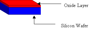
Select silicon wafer which is p-type substrate |
 |
2.
A layer of silicon oxide is grown on the wafer |
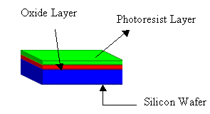 |
3. A solution of the polymer
resist is spun on the oxide layer and then the wafer is baked to remove
the solvent; thus to form a thin film |
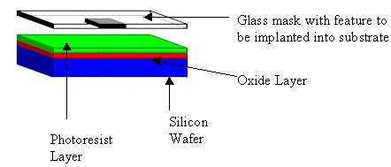 |
4.
The semiconductor design can be implemented by utilizing a pattern
mask and exposing it to a homogenous radiation source, or design pattern
can be directly written on the resist. In this case we will
use a glass mask to pattern. |
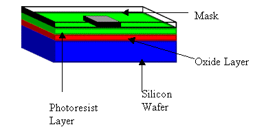 |
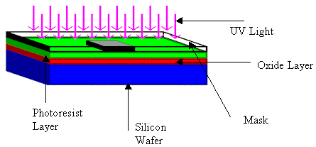
5.
Once the mask is properly aligned on the resist, the substrate is
ready for exposure. The mask is designed in a such a manner
that it contains transparent and non-transparent areas; thus
upon exposure, light passes through transparent areas of the mask
and is absorbed by the photoresist, while the non-transparent areas of the mask
absorbs the light, and keeping that area of photoresist
unexposed. |
 |
6.
Chemical properties of the photoresist material
changes when it is exposed to any type of
radiation source (e.g. UV light). Photoresist
can be classified as positive, meaning degradation of the polymer
resist upon exposure, and negative meaning the crosslink of the polymer
upon exposure. |
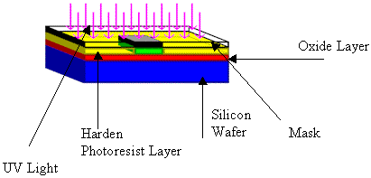 |
7.
The part of the photoresist that was exposed
to the radiation source is hardened (yellow), while the chemical properties
of the unexposed photoresist stays
the same (green). |
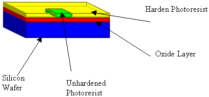 |
8.
After the exposure the pattern mask
is lifted for etching.
The feature to be etched is 'imaged' by unhardened photoresist. |
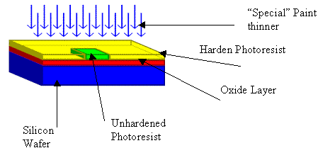 |
9.
To etch the unhardened resist, the
substrate is exposed to " 'special' paint-thinner" which
is a photoresist solvent; therefore where exposed to radiation,
it resists solvent |
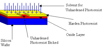 |
10.
In this step, solvent for the unhardened
photoresist is applied in order to etch the unhardened photoresist |
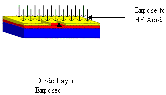 |
11. After
etching of the photoresist the substrate
is expose to Hydrofluoric Acid to etch the
oxide. In this step the resist layer acts as a mask. |
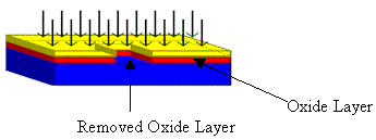 |
12. Since
the polymer photoresist 'resists' the hydrofluoric
acid, exposed oxide layer is etched by HF acid. |