Electron beam lithography (EBL) is a technique for creating extremely fine patterns (sub micron patterns, 0.1m m and below) for integrated circuits. This is possible due to the very small spot size of the electrons whereas the resolution in optical lithography is limited by the wavelength of light used for exposure. The electron beam has wavelength so small that diffraction no longer defines the lithographic resolution. EBL
finds applications in the following areas:
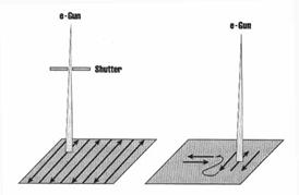
1. E-Beam Lithography Systems: Figure 1: Electron Beam Writing Strategies Direct write EBL systems are the most common EBL systems.
Most direct write systems use a small electron beam
spot that is moved with respect to the wafer to expose the wafer one
pixel at a time. Direct write systems can be classified as raster scan
or vector scan, with either fixed or variable beam geometry. Figure
2: A comparison
of scanning methodolgies; raster scan (left)
and vector scan (right) Figure 3 : Schematic of an electron-beam exposure system Several
versions of projection and proximity EBL systems have also been developed.
The short penetration length of electrons precludes the use of a solid
substrate like quartz for the mask, however. A very thin membrane mask
can be used, or else a stencil mask with cutouts through which beam
can pass is needed. These mask difficulties are sufficient to make projection
and proximity e-beam an unattractive technology for IC manufacturing. As
can be seen from the picture above all electron beam exposure systems
have four main subsystems: (1) electron source (gun), (2) electron optical
column (the beam- forming system), (3) mechanical stage, and (4) the
computer used to control the various machine subsystems and transfer
pattern information to the beam deflection coils. 2. E-Beam Resists: Electron
beam resists are the recording and transfer media for e-beam lithography.
The usual resists are polymers dissolve in a liquid solvent. After baking
out the casting solvent, electron exposure modifies the resist. As in
optical lithography, there are two types of e-beam resists: positive
tone and negative tone, with the usual behavior i.e., positive resists
develop away at exposed regions whereas in the case of negative resist
the developed region remains behind after development. Positive
e-beam resists undergo main-chain scission when exposed to e-beam as
shown below for PMMA. Figure
4: Mechanism
of radiation-induced chain scission in PMMA On the other hand negative e-beam resists function on the
basis of radiation-initiated cross-linking reactions that result in
the formation of interchain
linkages, which generate a cross-linked, three-dimensional network,
which is insoluble. The cross linking mechanism for COP is shown below. Figure
5: COP,
Some
of the positive e-beam resists are:
PMMA (Poly methyl methacrylate), EBR-9 (another acrylate based resist), PBS (Poly butene-1-sulphone),
ZEP (a copolymer of a -chloromethacrylate and a -methylstyrene). And
some of the negative tone e-beam resists are
: COP ( an epoxy
copolymer of glycidyl
methacrylate and ethyl acrylate) and Shipley SAL (has 3
components, a base polymer, an acid generator, and a crosslinking agent).
Figure
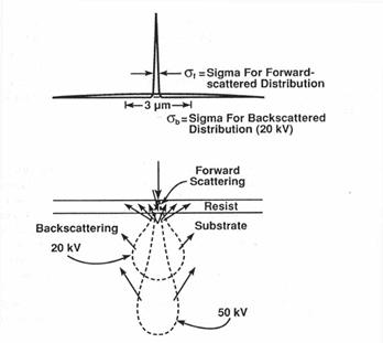
6: 3. Electron Solid interactions: As
the electrons penetrate into the resist material some of them experience
small angle forward scattering and many of them experience large angle
scattering events leading to backscattering. This causes additional
exposure in the resist leading to what is called the electron beam proximity
effect. As the primary electrons slow down, much of their energy is dissipated in the form of secondary electrons with energies from 2 to 50 eV. These are responsible for the bulk of actual resist exposure process. Since their range in resist is only a few nanometers, they contribute little to the proximity effect.
A
small fraction of secondary electrons may have significant energies,
on the order of 1 keV.
These so-called fast electrons can contribute to the proximity effect
in the range of few tenths of a micron. Figure
7: Electron
scattering in electron resist exposure 4. Modeling: Electron trajectory: The
fundamental parameter necessary to determine developed resist profile
is the absorbed energy density and its dependence on spatial position
within the resist film. The
Where a0 = Bohr radius (0.53 A° ), and Z is the atomic number of
the element. From
this atomic potential, the differential scattering cross-section per
unit solid angle is given by the
Where m is the mass of electron, v its velocity, Zi the atomic number
of the ith
species, a i is the atomic screening
parameter.
Where E is the energy
of the incident electron. Between
elastic scattering events the electrons are assumed to travel in straight
lines (of length equal to the mean free path) and undergo energy loss.
The energy loss is modelled
via the CSDA (continuous slowing down approximation) according to the
Bethe energy loss formula,
where ne
is the density of atomic electrons, I is the mean excitation energy,
a is constant equal to 1.166. Within
the step length the electron is assumed to have a constant energy Eo.
The electron energy at point 1 is then calculated by decrementing the
energy with respect to its value at point 0 via the Bethe expression for energy loss per unit distance.
(The sequence is repeated continuously until the energy has degraded
to some arbitrary value close to the mean ionization energy). By carrying out many such simulations, trajectory patterns
can be generated, and an absorbed energy matrix E(r,z)
can be calculated. Figure
8: Geometry
for Figure 9: Monte Carlo simulated trajectories of 100 point-source in a target of 1 um thick resist on silicon substrate at 10 (a), 25 (b), and 50 (c) keV incident energy.
5. Development Modeling: The
developed resist profile depends not only on the absorbed energy density,
but also on the development process itself. An ability to predict resist
profiles as a function of the exposure parameters therefore requires
development models integrated with the exposure models. There is usually
a change in molecular weight for a given e-beam exposure level given
by (for a positive resist),
Where r is the resist density, A0 is the Avogadros number, G(s) is the number of scissions per 100eV
of absorbed energy, Mn0 is the original number
average molecular weight, and Mf is the final number average
molecular weight (less than Mn0). Knowing
the change in molecular weight for a given exposure level and the dependence
of solubility on fragmented molecular weight, the 2-D E(r,z) can be transformed into the solubility rate matrix,
and the profile can be determined as a function of development time.
For PMMA resists Greeneich
has examined these effects using an empirical equation.
where R0, b , and a are empirically determined constants
that depend on the developer used.
Figure
10: Actual PMMA Resist Profiles at an incident
charge density of 10-4 (a), 8e-5 (b), and 5e-5 (c) C/cm2. 6. References: 1. Rai-Choudhury, P. "Handbook of Microlithography, and Microfabrication, " Spie Optical Engineering Press, 1994. 2. Thompson, Larry; Wilson, Grant; Bowden, Murrae; "Introduction to Microlithography," Second Edition, 1994. 3.
Campbell, Stephen. "The Science
and engineering of Microelectronics Fabrication," Oxford University
|